Integrated circuits (or ICs) provide the computational power that drives modern electronics and electrical devices, from the phones in our pockets to telecommunication satellites orbiting the Earth. The technology that makes all of this possible is certainly impressive, but the semiconductor manufacturing plants and systems that produce these microelectronics are nothing short of manmade miracles.
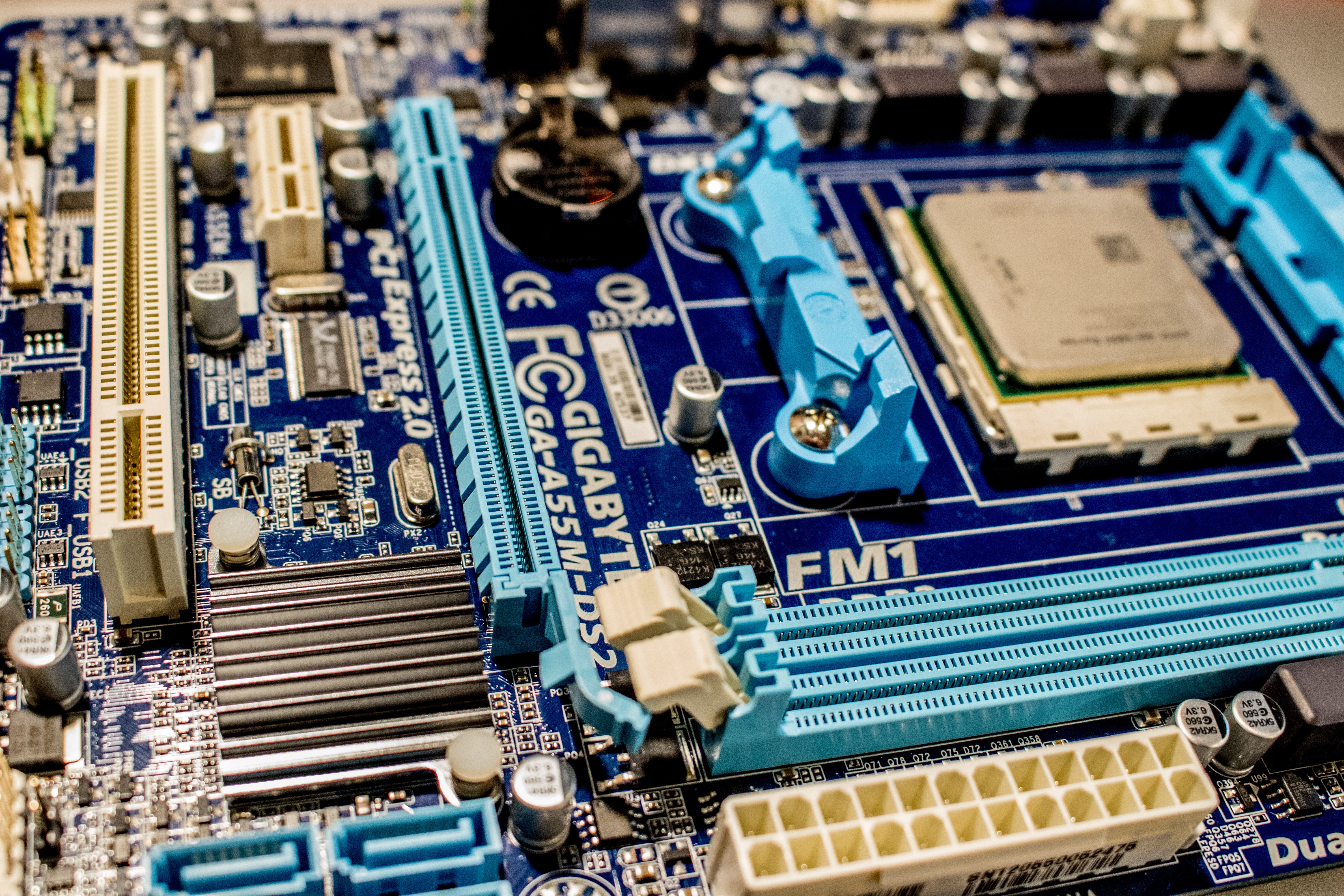
Semiconductor manufacturing transforms raw silicon, polymers, and metallic materials into electrical transistor switching wafers using production equipment and processes that operate in spaces measured in nanometers. At this scale, precision, accuracy, and fidelity are of the utmost importance. Production runs can be entirely scrapped by singular dust particles that contaminate wafer boards, or even transient moisture in the air that causes circuit paths to electrically short out. For these reasons, production system cleanliness, integrity, and reliability are paramount, which brings us to the role of ultra-high quality process controls and instrumentation in meeting these demands.
Instrumentation Applications in Semiconductor Production
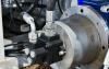
Multiple steps in semiconductor manufacturing rely on automated fluid, gas, vacuum, and thermal systems to perform within exacting tolerances, repeatedly across millions of cycles. In particular, precision instrumentation acts as a process control systems' sensory connection to the work in progress, providing real-time data used for instantaneous automated decision making to keep production moving smoothly. Instruments must not only have the accuracy and dependability to perform as expected, but also must be constructed in ways that will withstand the environments in which they're located. High temperatures, aggressive chemicals, corrosive medias, and rigorous cleaning are all par for the course.
Below we'll provide a few examples of semiconductor manufacturing applications, each presenting unique demands onto their control system’s sensors.
- Wafer Processing - wafer printing calls upon many fluid and gas systems throughout the course of turning silicon and conductive ions into powerful transistor arrays, requiring robust instrumentation such as level transmitters for acetone cleaning reservoirs, pressure transmitters for photolithography coating dispensers, and vacuum switches for vacuum vapor deposition.
- Die Processing - dicing individual dies from larger wafers and size forming (such as through back-grinding or edge square trimming) generates refuse material that must be actively removed by vacuum systems and / or inert gas purge systems, which require pressure and vacuum instrumentation to operate appropriately.
- IC Packaging - encapsulating the die into its final housing completes the manufacturing process, and can be the most critical step towards assuring chip performance and long life. This process involves vacuum particulate capture and pressurized inert gas purge systems again, as well as flow transmitters and switches for adhesive and coating dispensing.
- Process Support Systems serve production equipment with imperative services such as Ultrapure Water, Dust Collection, Vacuum Evacuation, Bulk Chemical Distribution, and Cooling / Heating / Refrigeration Thermal Maintenance. These systems use all varieties of industrial instruments and switches.
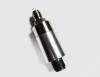
When selecting instrumentation for microelectronic applications, buyers must fully consider performance and construction specifications against their exact requirements. Beyond the accuracy and repeatability of an instrument's circuitry, housing materials, process connection types, wiring specs, and certifications are important factors in selecting the ideal sensor. Stainless steel type 316 or above housings, metric BSPT fittings, and shielded 4-20mA output (for transmitters) or NPN (for switches) circuits are common selections for these projects.
Central Plant Utilities
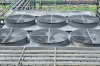
Beyond the incredibly complex equipment used to produce microelectronic products, semiconductor plants also house some of the most robust utility infrastructure systems in modern industrial manufacturing. All mechanical, electrical, thermal, and fluid services that the fabrication equipment needs to operate come from a separate area of the plant, typically known as Central Utilities. These utility systems utilize process control and instrumentation of the same (if not better) quality as used in the fabrication process. More so, modern concerns around sustainability and energy efficiency drive even higher caliber control needs, specifically in water and thermal systems that are the most energy intensive.
Water Recycling and Reclamation
While traditional semiconductor plants reuse approximately 40 to 70 percent of their daily water consumption (which can easily hit millions of gallons per day in large plants), emerging new technologies can bring that figure as high as 98% reuse using advanced treatment, filtration, and polishing techniques. These systems rely on accurate pressure, temperature, flow, and level transmitters, to name a few items.
Sterile-Grade HVAC
Chip manufacturing equipment requires extremely clean environments, and building air handling and ventilation systems play an integral role in keeping airborne particulates, vapors, and odors out. Clean-room sterile air handling systems utilize precise pressure and temperature transmitters, in particular.
Central Laundry
Clean room environments call for a healthy level of caution around ingress of foreign contaminants, and one key way that this is managed is by enveloping employees in protective outerwear. Gowns, hoods, smocks, booties, and gloves all were disposable in years past, but have evolved into reusable variants that can be laundered to substantially reduce waste. In-plant laundries use central steam, water, and chemical systems, all of which use a wide array of online pressure, temperature, level, and vacuum instrumentation.
Semiconductor Manufacturing of Tomorrow
The cutting edge of IC production is akin to the Wild West of engineering and physics, racing to the extreme bottom of material science to the tune of field-effect transistors assembled at the atomic level. Further, these nanoelectronic circuits are printed on increasingly large wafer sizes, and now - incredibly - in three dimensions (whereas traditional transistors have all been two-dimensional designs). The concept of circuits this small and in such density takes electronic engineering into the realm of quantum mechanics, and the leading technologists driving this industry forward are far from finished. Where their designs go, precisions instrumentation used in these manufacturing solutions must follow.
As a veteran-owned small business, Whitman Controls is dedicated to supplying premium quality, reliable, technologically advanced instrumentation for use in nearly any application. Our Bristol, CT manufacturing facility embodies over 40 years of engineering, fabrication, and customer service expertise, serving both end-user and manufacturing customers nationwide through direct and distribution channels. Our values drive us to provide the highest level of servant partnership that you can find. To discuss your applications or to learn more about our capabilities, please contact us at (800) 233-4401, via email at [email protected], or online at www.whitmancontrols.com.